
Crossbar, the resistance RAM (RRAM) startup, opened the kimono a little wider today with the announcement of their “1TnR” architecture, which they have implemented on pre-production test chips.
Unpacking 1TnR: 1 Transistor drives n number of RRAM cells. How many? They report that a single transistor can drive over 2,000 memory cells at very low power and super density.
How dense? They say 1TB on a single die, with 3D stacking of memory cells. Point: this is on-chip deposition of multiple layers of memory cells, not the mechanical 3D of NAND flash that requires VIAs and precise positioning of multiple dies.
Pictures
The Crossbar memory cell uses a metallic nano-filament in a non-conductive layer that can built on current CMOS fabs. Here’s a Crossbar diagram showing the cell’s various states:
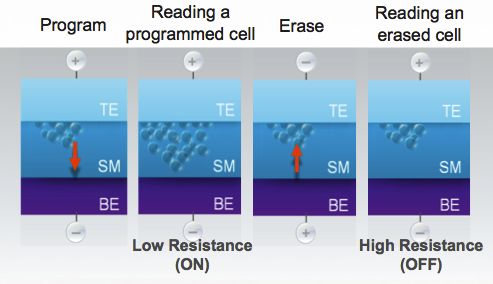
TE = Top Electrode
SM = Switching Medium
BE = Bottom Electrode
As StorageMojo related last week Crossbar co-founder Wei Lu, a Michigan professor, made a breakthrough discovery in how their RRAM works: it moves metal particles through a solid. That’s new.
The StorageMojo take
Crossbar is in the process of licensing its technology to some major fabs. The simplicity and scalability of its process means it can be built on fully depreciated CMOS lines using old technology. Large feature sizes aren’t a big problem when you can stack multiple cell layers on a single die.
Commercial shipments are planned for 2017 assuming all goes well. But if the cost and density predictions pan out, Crossbar’s RRAM will be a game changer for SSDs, NVDIMMs and, eventually, enterprise storage. Keep an eye on them.
Courteous comments welcome, of course. What other info would you like to see from Crossbar?

Recent Comments